

Flexible Printed Circuit Board (FPC) – Innovation in Electronics Industry
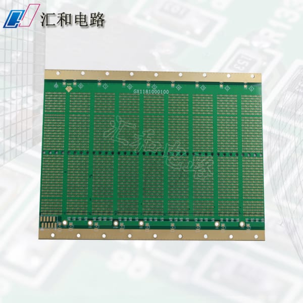
The Electronics industry is witnessing dramatic transformations with the development of flexible printed circuit boards (FPC). These boards are taking the place of the traditional rigid printed circuit boards (PCB) due to their flexibility, reduced weight, and space-saving capabilities. FPC boards are essential parts that connect electronic devices’ components and transmit the electrical signals between them. This article delves into the world of FPC boards, discussing what they are, their advantages, limitations, and applications.
FPC board – What is it?
A flexible printed circuit board (FPC) is a type of PCB with various layers of conductive material embedded between two layers of flexible polymer film. The layers of conductive material are interconnected with vias to create electronic circuitry. The polymer film allows the board to be bent or folded without cracking, making it an excellent option for creating complex circuit designs in smaller devices.
Advantages of FPC Board
The primary advantage of the FPC board lies in its flexibility. As mentioned earlier, the FPC board provides the ability to bend, twist, and fold circuits that traditional rigid PCBs cannot withstand, making it ideal for complex and intricate designs. Additionally, FPC boards have a lower weight and smaller footprint than rigid PCBs, making them ideal for applications requiring space optimization, such as wearable electronics, smartphones, tablets, and other consumer devices.
FPC boards also offer excellent performance in high-temperature environments. Their heat-resistant polymer film and conductive materials make them less sensitive to high temperature over extended periods. This feature makes them suitable for aerospace, military, and automotive applications.
Limitations of FPC Board
As with any technology, FPC board also has some limitations to consider. One of the main constraints with FPC boards is their complexity. Due to their flexibility, FPC boards have intricate circuit designs that demand significant expertise for manufacturing, making their cost per unit higher than that of traditional PCBs. Additionally, FPC boards’ flexibility also means they cannot handle as much power as rigid PCBs, restricting their use in high-power applications.
Applications of FPC Board
FPC boards have found their way into many applications, including those that require a flexible form factor. For example, the medical industry uses FPC boards on respiratory devices, drug delivery systems, and body monitoring systems. The automotive industry also benefits from FPC boards, using them in electronic control units (ECUs), sensors, and lighting systems in vehicles.
FPC boards are also prevalent in the consumer electronics industry, such as smartphones, tablets, laptops, and smartwatches. They provide a compact and space-saving solution, allowing for thinner foldable designs, larger screens, and extended battery life. In the aerospace and military industries, FPC boards have found use in avionics, satellite communication systems, missile systems, and other electronic-based applications.
Conclusion
The advent of flexible printed circuit boards (FPC) has opened up new possibilities for electronics design, leading to smaller, more efficient, and more complex devices. By overcoming the limitations of rigid PCBs, FPC boards have expanded their applications to a broad range of industries, including automotive, aerospace, consumer electronics, and medical devices. FPC technology is continuously evolving, with more advanced materials, efficient component placement techniques, and low-cost manufacturing processes emerging. With all these improvements, the future looks promising for FPC technology.
相關新聞
-
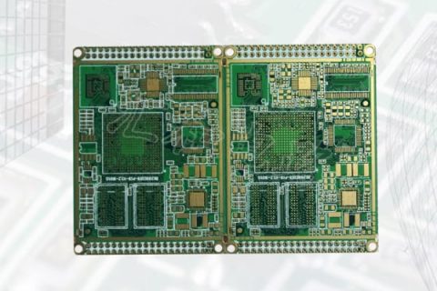
pcb八層板疊層結構,pcb八層板如何分布層?
隨著科技的不斷發展和進步,PCB(印制電路板)已經成為現代電子制造中不可或缺的一部分。而在眾多的PCB形式中,八層板是應用廣泛的一種。 PCB八層板疊層結構 八層板是指在印制電路板的頂層和底層各有一層電路層,中間有6層地面層和電源層。這種結構一方面可以提高電路板的穩定性和可靠性,另一方面還可以大大降低電磁噪聲和電磁干擾。在實際應用中,八層板主要用于高速信號傳輸和復雜電路設計中。 PCB八層板分布層 在設計PCB八層板分布層時,需要考慮以下幾個方面: 1. 信號層和電源層的分布 為了保證信號傳輸的…
-
pcb表面處理工藝有哪些,pcb表面處理工藝有幾種方法?
PCB表面處理工藝是電路板生產過程中不可或缺的一個環節,其目的是在PCB表面形成一層保護層,以增強電路板抗氧化、耐久性能,同時使電路板表面達到某種特定的幾何形態和表面形貌,以方便后續的工藝加工和電路測試。那么,PCB表面處理工藝有哪些呢?方法有幾種呢?本文將為讀者一一解析。 首先,PCB表面處理工藝可分為兩種:裸板表面處理和已焊接部分表面處理。 裸板表面處理工藝:1.化學陶瓷處理法這是一種將PCB表面通過化學陶瓷涂層的方法,實現PCB表面處理的方法。無鉛化化學陶瓷技術應用于焊盤和線路的表面處理,…
-
pcb焊盤工藝有幾種?
PCB焊盤工藝是電路板生產過程中非常重要的一環,它涉及到電路板的成型和接線安裝問題,非常關鍵。隨著電子產品的廣泛應用,對電路板的生產需求不斷增加,因此掌握不同種類的PCB焊盤工藝至關重要。在本文中,我們將介紹不同種類的PCB焊盤工藝,以幫助讀者更好地了解和掌握該技術。 1. 表面貼裝(SMT) SMT(Surface Mount Technology)是目前最常用的一種PCB焊盤技術,它是以SMD元器件為代表的一種焊盤技術。SMT焊盤工藝不需要通過孔,而是直接焊接在PCB表面。與傳統的孔式焊盤工…
-

pcb過孔最小多少,pcb過孔有什么用?
PCB過孔指的是印刷電路板(PCB)上的穿孔,一般用來連接電路板上不同的層級,以便傳遞信號與電力。但是,在PCB過孔的設計與制造過程中,我們會遇到一個重要的問題,那就是其最小尺寸。本文將詳細探討PCB過孔的最小尺寸及其意義。 PCB過孔的最小尺寸究竟是多少? PCB過孔的最小尺寸是由生產工藝的限制來決定的。最小尺寸會影響PCB過孔的排列密度和板設計。過孔的尺寸要大于所需的導通電流的閾值。因此,根據電流閾值和板的厚度,總尺寸應該足夠大,通常大于供電電壓的兩倍。 對于貼片元件,建議使用0.3mm的最…
-
pcb拼版是什么意思,pcb拼板的規則和方法是什么?
PCB拼板是指將多個PCB設計文件拼接在一起,以便更高效地制造和組裝電路板。通常情況下,拼板是由CAD軟件完成的,但在實際生產中,需要根據一些規則和方法來完成。 PCB拼板的規則主要涉及到以下幾個方面: 1.板間距離規則在拼板時,必須考慮到電路板與電路板之間的間距,以便能夠更好地制造和組裝。PCB拼板時,通常要求板與板之間的距離保持在一定范圍內,以防止電路板之間的短路現象發生。根據業內的標準,板與板之間的距離通常應在2毫米到3毫米之間。 2.板材厚度規則電路板的厚度通常根據使用要求而選擇,但在P…
-
什么是pcb行業,什么是pcb設計?
什么是PCB行業,什么是PCB設計?這是許多人在了解電子行業,電路板制造等方面時會問的問題,而本文將為你詳細解答。 PCB行業是什么? PCB行業又稱為電路板行業,是指從電路板的設計、制造、組裝、測試等全過程,以及與之相關的材料、設備和技術服務等方面的產業鏈。隨著現代電子技術的迅猛發展和電子產品應用的日益廣泛,電路板制造作為電子產品中不可或缺的組成部分,具有巨大的市場潛力和前景。 PCB設計是什么? PCB設計是指以電路原理圖為基礎,在保證電路功能的前提下,按照規定的布局及線路連接方式,對電路板…
 3002788751